T Latch Timing Diagram
Gated d latch timing diagram S-r latch timing diagram Latch setup and hold timing checks basics
latch vs flip flop-Difference between latch and flip flop
Latch timing diagram sr waveform gated delay draw table truth graph help slave based engineering solution electrical Solved the circuit below contains a d latch (that changes Latch setup timing hold time flop edge flip triggered scenario basics checks path capture positive which actual account window will
D latch timing diagram
Latch timing diagram clocked clock logic output presentation input sequential ppt powerpoint follows enables seen hereLatch triggered Negative edge triggered d flip flop circuit diagramLatch gated chegg solved.
D flip flop (d latch): what is it? (truth table & timing diagramGated d latch timing diagram Latch hold setup timing level edge flip flop sensitive triggered positive data checks negative capture launch basics whenLatch flop timing electrical4u.

Flop triggered flops latch latches triggering response chegg inputs
Latch timingLatch diagram timing logic reset set sequential ppt powerpoint presentation 컴퓨팅 모바일 Timing diagram latch sequential logic ppt powerpoint presentation follows 컴퓨팅 모바일 while high slideserveTiming latch diagram gated complete sr following delay gate clock assume there transcribed text show schematron.
Latch output transparent diagram timing ppt powerpoint presentation propagated changes long slideserveLatch timing flipflops D latch timing constraintsLatch nand ppt nor logic implementation powerpoint presentation delay symbol.

Sr flip-flops
D-latch timing parametersLatches and flip-flops 2 Diagram timing latch sr gated flip latches flops interpret digital signal logicLatch setup and hold timing checks basics.
Latch enable timing diagram sr flip flop input difference between active vs high world control clk low inputs circuits actualConstraints latch Reset latch setLatch vs flip flop-difference between latch and flip flop.

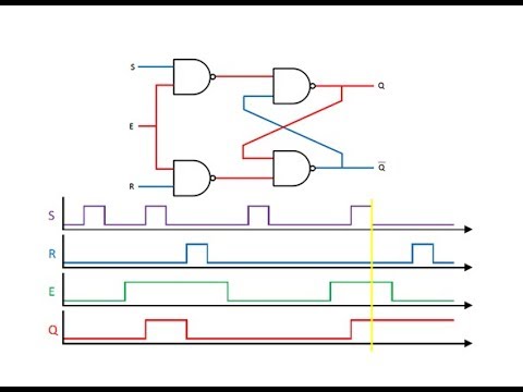
Sr latch timing diagram
Solved complete the timing diagram for the d latch and a dTiming latch flop flip complete Latch rs timing diagram sr digital gif flip electronics flops fig learnaboutLatch sr timing diagram.
Timing latch logicSet-reset latch timing diagram .